
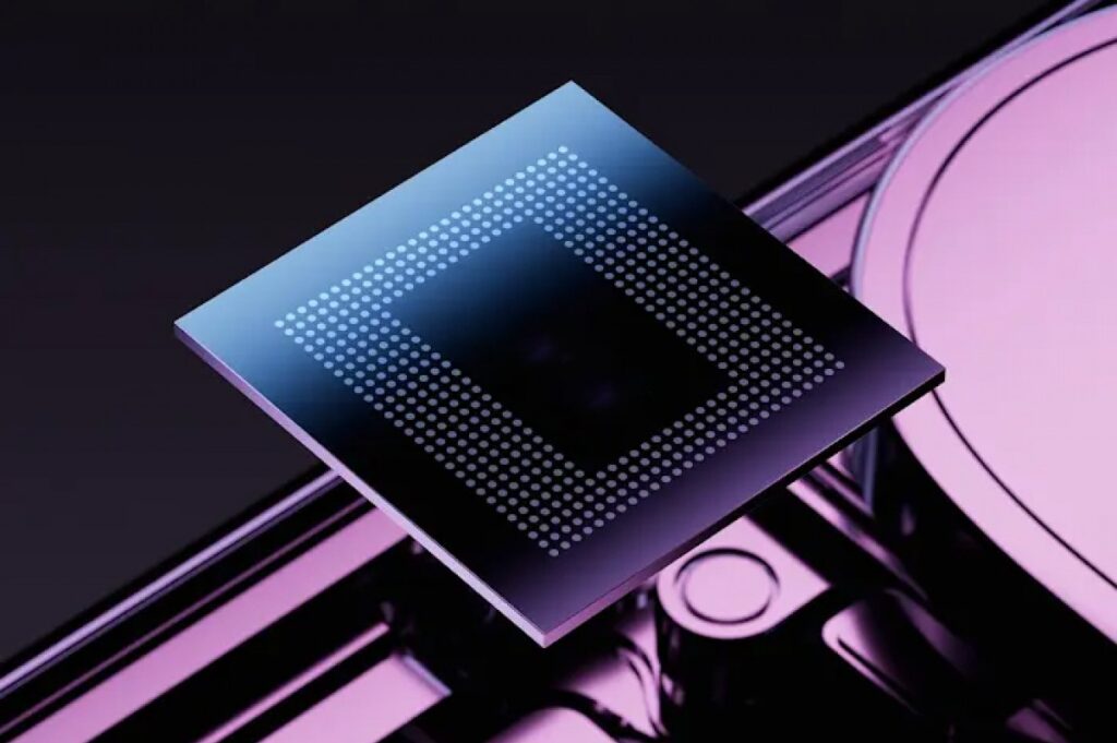
A recent report from Android Authority reveals details about the forthcoming Tensor G5 chipset, which will drive Google’s upcoming Pixel 10 series. Significantly, Google is switching from Samsung to TSMC’s 3nm-class technology for chip production and is introducing a fully in-house Image Signal Processor (ISP).
Custom ISP
A standout feature of the upcoming chip is its fully custom image signal processor (ISP), marking a first for Google’s in-house chip development. Previously, Google utilized a hybrid design that combined Samsung’s ISPs with some of its components. This significant change hints that the Pixel 10 series may experience a considerable transformation in camera performance, whether for better or worse.
New GPU
Additionally, Google is replacing the Arm Mali-G715 MP7 GPU from the Tensor G4 with a GPU from Imagination Technologies, specifically the IMG DXT. The extent of this upgrade remains uncertain, and we will need to wait for reviews to find out more.
In addition to the GPU and ISP enhancements, Google plans to introduce a custom memory controller and system-level cache, along with new power modules that have not been featured in earlier Tensor versions.
More Third-Party Friendly
The chip is also expected to incorporate third-party components for USB, PCIe, and I3C, as well as interfaces for display (DSI, DisplayPort) and storage (LPDDR5x flash memory).
Furthermore, Google will move away from its proprietary “BigWave” AV1 codec and Samsung’s MFC (Multi Format Codec), opting instead for Chips&Media’s WAVE677DV, which can encode and decode AV1, VP9, HEVC, and H.264 formats. This represents another shift in collaboration for Google as it refines the Tensor G5 into a more cohesive and third-party-friendly platform.
For more daily updates, please visit our News Section.